I implemented a 16-bit RISC processor using logic gates.
The Arithmetic Logic Unit. The Instruction Decoder. The Program Counter. The Register File. The Flag Register. And the bus connections between these.
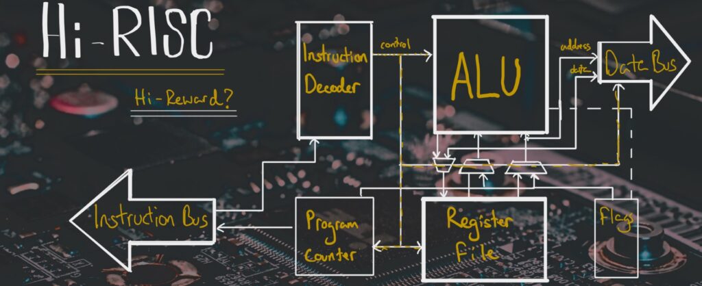
I designed the CPU using Hardware Description Language (HDL), creating individual modules for each component and integrating them into a complete system. I wrote assembly code in a text editor, assembled it with the HF-RISC assembler, and performed data manipulation and mathematical operations, running my CPU design on an FPGA.
RISC -> AVX512??
Working as a software engineer at Parallel Wireless required a deep understanding of how CPUs operate to maximize performance — given 5G’s demands for high data rates and ultra-low latency. Although the CPU I developed is far simpler than the modern ones used at Parallel Wireless, this project significantly enhanced my ability to conceptualize complex processors and identify inefficiencies – for instance due to cache misses or branch misprediction. As a result I was able to implement very optimised code. My Matrix Inversion algorithm even outperformed the highly-optimised Matrix Inversion algorithm from ARM RAN Acceleration Library… on ARM’s very own CPUs.
Semiconductors are awsome
CPUs are beautiful and powerful things. They have undoubtably changed the course of human history, ushering in the age of information. I highly-recommend the book “Chip Wars”, which walks you through the birth and growth of the semiconductor industry and the role it plays today. The race for the most advanced chips has become central on the global political stage. Nations like the United States and China are investing hundreds of billions to secure a computational edge, recognizing that military superiority is increasingly tied to technological prowess. Beyond geopolitics, leading companies also rely on cutting-edge computational power to stay competitive in an ever-evolving digital landscape.
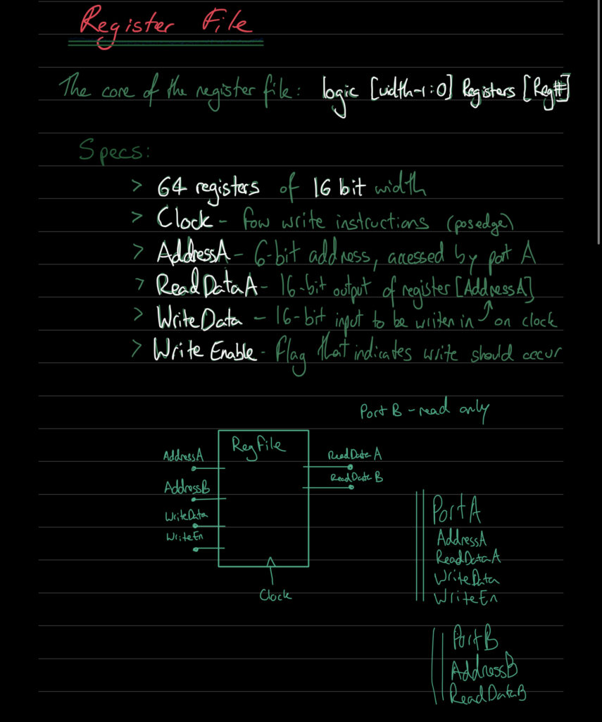
Processor specs
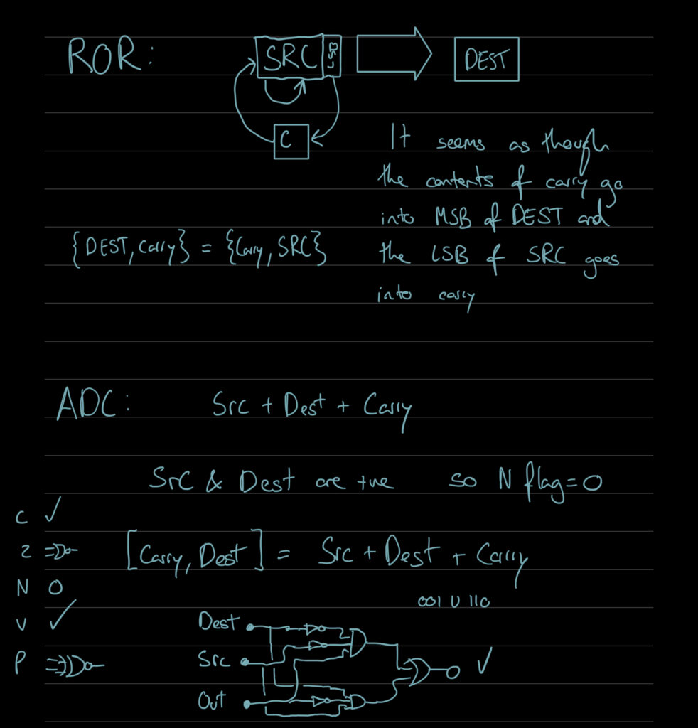
This 16-bit processor had an instruction set which could do bitwise logic, integer arithmetic, and data manipulation. It decoded the instructions – of which there were 16 – and passed the control signals to the ALU or the registers depending on the instruction. There was a main register file which could hold up to 62 words (16-bit words). There was a flag register – holding 6 flags that were affected by results of operations. And there was a program counter – keeping track of what instruction to execute next.
Future improvements
The next step would be improving the pipelining. By improving the control unit I could have multiple instructions executing at the same time. This would not improve latency – instructions will still take a cycle to process – but the throughput (IPS) could be greatly increased. This would be implemented by starting the next instruction before the last is finished while not using the same resources. Branch prediction would need to be implemented too – as otherwise the program would not know what instructions are (likely) safe to load next.
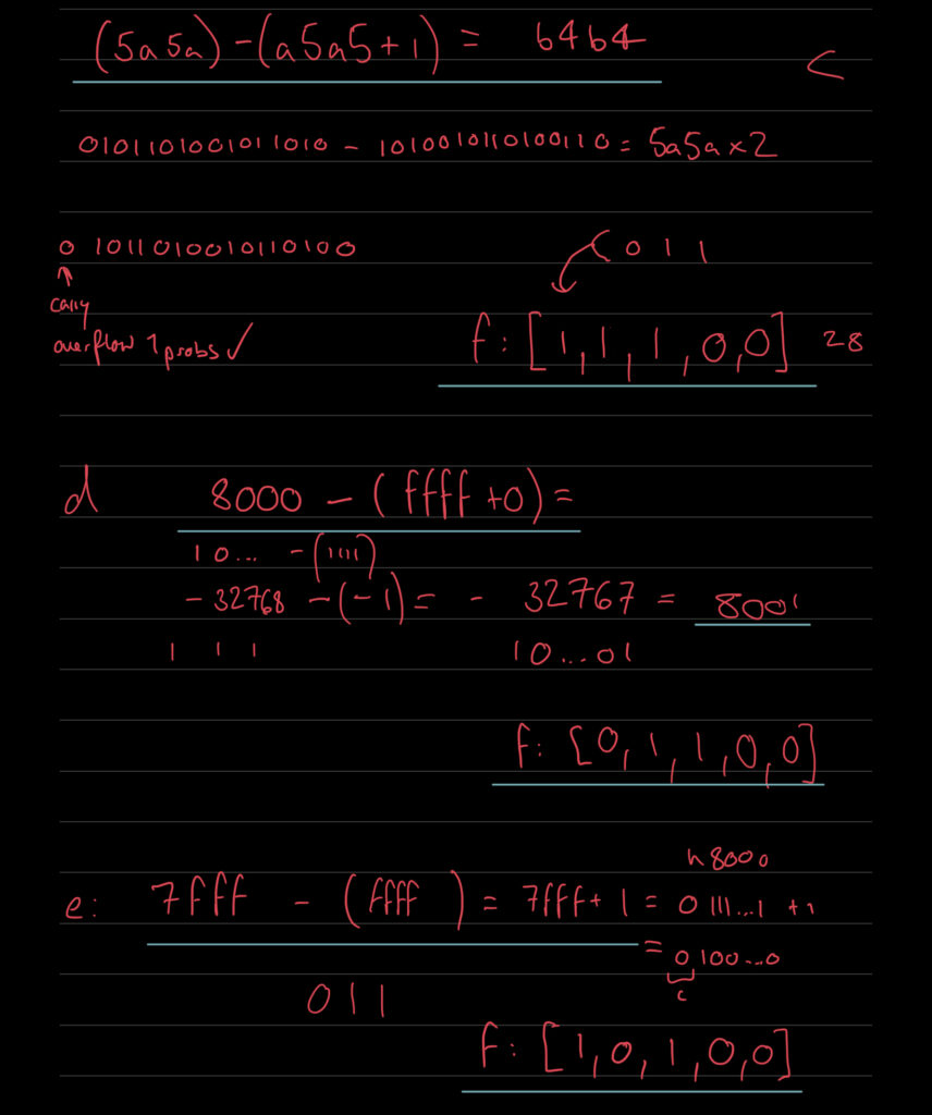
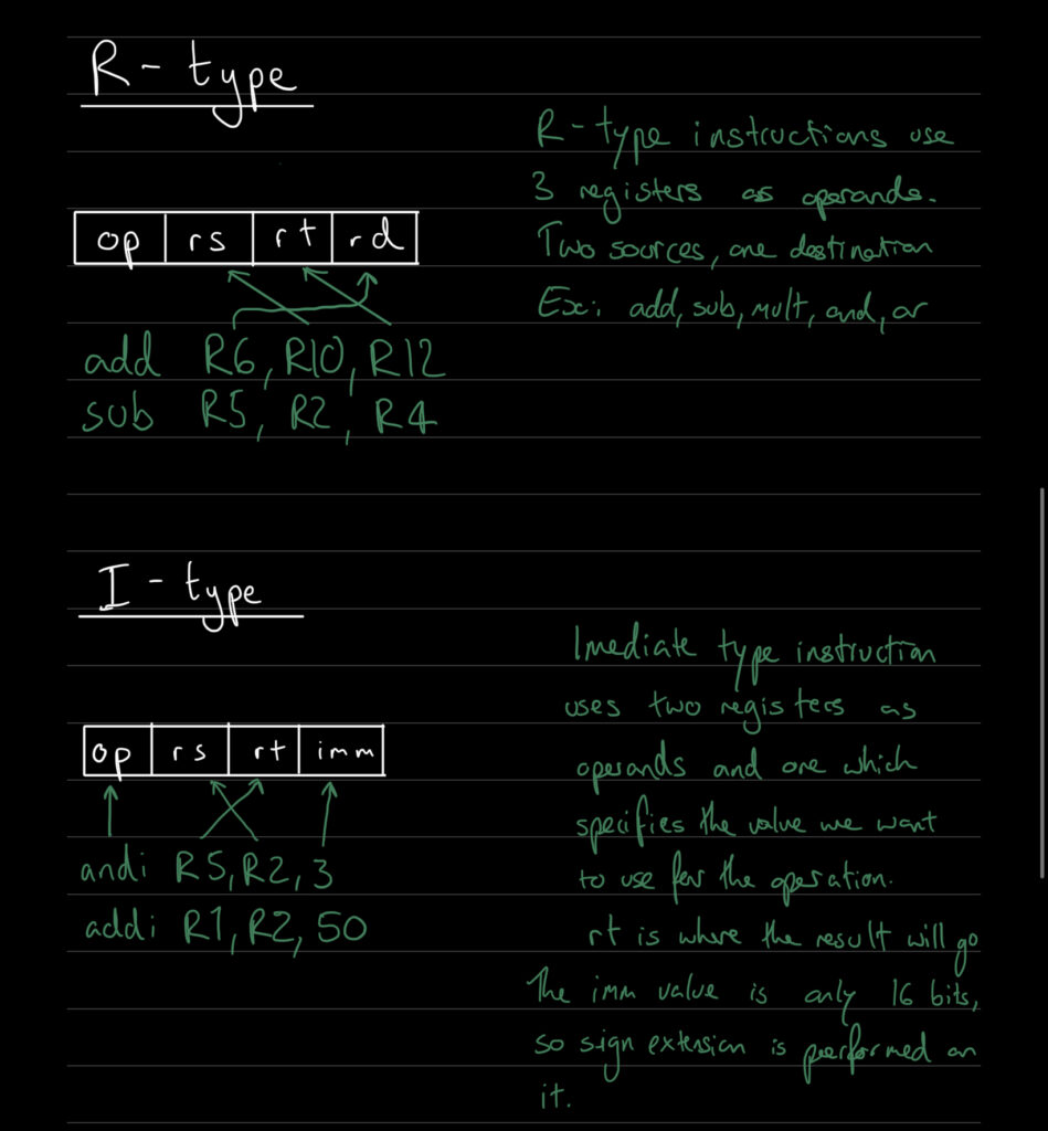
(Some old notes from when I was designing it:)